Fine-Pitch Precision: Electronics Stamped Electrical Terminals Engineering Guide
A 0.4 mm pitch connector that passes AOI can produce intermittent open circuits after SMT reflow — terminals with coplanarity drift of 0.08 mm break solder joints during shipping vibration. The rework cost on a 12-layer PCB exceeds the connector price by 100x.
In this guide, you will learn coplanarity control for fine-pitch stamped terminals in SMT connectors. You will also find J-STD-001 solderability qualification and signal integrity validation above 5 Gbps.
Read on for the full engineering guide.
SMT Assembly Interface
Lead Coplanarity and Solder Joint Formation
Electronics terminals destined for surface-mount assembly face a multi-dimensional tolerance challenge that begins at the stamping die and ends at the reflow oven. A connector with 40 SMT leads in a dual-row 0.5 mm pitch configuration requires every lead to sit within 0.10 mm of a common seating plane after forming.

A terminal that is 0.12 mm above the plane — a deviation of 20 µm beyond the specification — may still make physical contact with the solder paste deposit during placement.
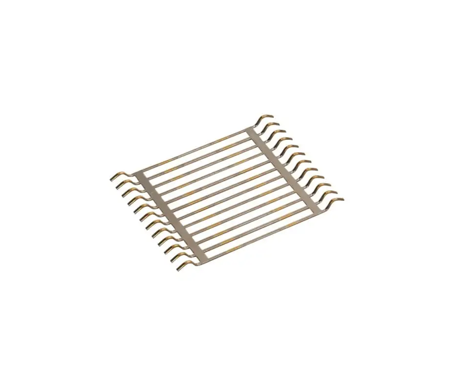
But during reflow, as the solder paste melts and collapses from its 0.15 mm printed height to a 0.08 mm fillet, that terminal lifts above the molten solder surface. The resulting open circuit passes visual inspection because the terminal and the pad both appear wetted, and the gap between them is hidden beneath the connector body.
Coplanarity variation originates from three sources within the stamping process. Material springback during forming introduces 0.02–0.05 mm of deviation depending on the alloy’s yield strength and the bend radius-to-thickness ratio.
Progressive die wear over 1–2 million strokes gradually shifts the forming punch position by 0.01–0.03 mm before the tool maintenance cycle resets it. Plating thickness variation of ±0.5 µm across the terminal strip changes the effective lead thickness by 1 µm — negligible as a single contributor but additive to the springback and tool wear components.
Controlling these three sources to maintain 0.10 mm total coplanarity requires in-die monitoring of the forming force signature, which detects springback variation before it produces out-of-spec terminals.
[Compliance Anchor]: SMT terminals for connectors with 0.5 mm pitch or finer must demonstrate coplanarity within 0.10 mm across all lead positions per JEDEC JESD22-B108, verified by 3D laser profilometry on a statistical sample per ANSI/ASQ Z1.4 from each production reel — 2D vision inspection cannot measure the Z-axis deviation that causes solder opens.
💡 Coplanarity Verification Gap: 2D AOI detects missing terminals but cannot measure the Z-axis deviation that starves solder joints — a 0.08 mm coplanarity drift produces opens that escape connector-level testing. request a coplanarity capability study for your terminal geometry before locking the stamping supplier.
Electronics Qualification Standards
Solderability Verification and Shelf-Life Risk
The IPC family of standards governs electronics assembly quality and forms the terminal supplier’s qualification baseline. IPC-A-610 defines the acceptability criteria for solder connections, and the terminal’s contribution to solder joint quality depends on solderability — the ability of the terminal surface to be wetted by molten solder within a specified time.
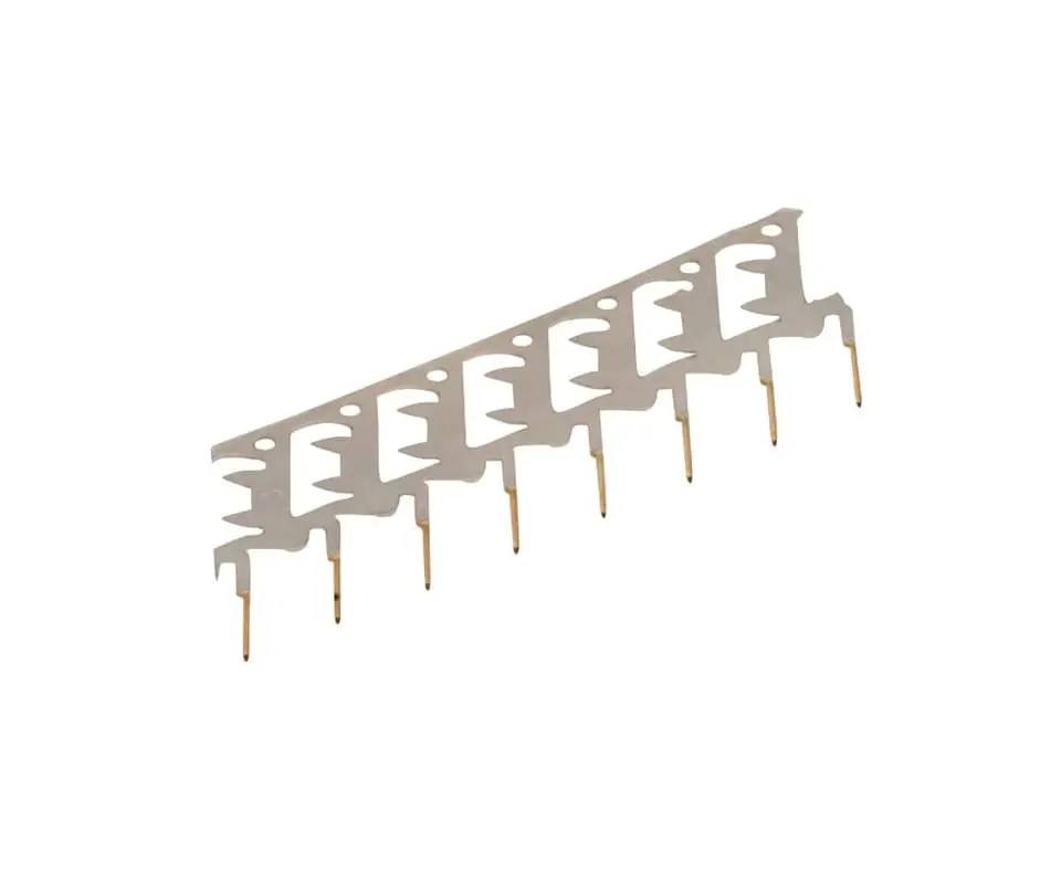
J-STD-002 quantifies this through a dip-and-look test: after 8 hours of steam aging to simulate the oxidation that occurs during warehouse storage, the terminal is dipped in SAC305 solder at 245°C, and the wetted area must exceed 95% of the solderable surface within 2 seconds.
Terminals that pass this test as-plated may fail after 6 months of storage if the tin plating’s organic brightener degrades under ambient humidity, forming a non-wettable surface film.
Signal integrity has become a terminal-level concern with the rise of PCIe Gen 4/5, USB 4, and HDMI 2.1 interfaces operating above 10 Gbps. At these data rates, a 1 mm stub on the terminal’s SMT lead acts as an unterminated transmission line stub that creates a resonance null in the insertion loss curve.
The terminal’s formed geometry must minimize the electrical length of any branch from the signal path, typically by transitioning the terminal from the contact point to the board-mount lead in a continuous curve rather than a discrete bend that creates an impedance discontinuity.
Time-domain reflectometry measurements on the production connector assembly detect these discontinuities as impedance peaks above 110 ohms or dips below 85 ohms from the 100-ohm differential target.
For electronics metal stamping in high-volume consumer applications, the qualification burden extends to process capability. A connector manufacturer shipping 10 million units per year needs a terminal supplier whose process Cpk exceeds 1.67 for critical characteristics — contact gap, insertion force, and coplanarity — demonstrated over a minimum of three production lots of 125 samples each. A supplier who can only demonstrate Cpk of 1.33 during qualification will drift below 1.0 within 6 months of production as tooling wear accumulates.
[Compliance Anchor]: Electronics terminal solderability per J-STD-002 must be verified on production-representative samples from each plating lot after 8 hours of steam aging, with a minimum of 95% wetted surface area within 2 seconds at 245°C — testing only as-plated terminals without steam aging passes terminals whose plating performs adequately fresh but degrades below the solderability threshold during the 6–12 month shelf life typical of connector inventory management.
Consumer & Industrial Stamped Terminal Archetypes
Board-to-Board and USB-C Connector Terminals
Board-to-board mezzanine connectors represent the precision frontier for electronics terminals. A 0.4 mm pitch connector stacking two PCBs at a 3 mm board-to-board distance places the stamped terminal under simultaneous constraints: the contact beam must generate 0.3–0.5 N of normal force on a 0.15 mm diameter pin while the SMT lead must achieve 0.10 mm coplanarity across 60 positions.
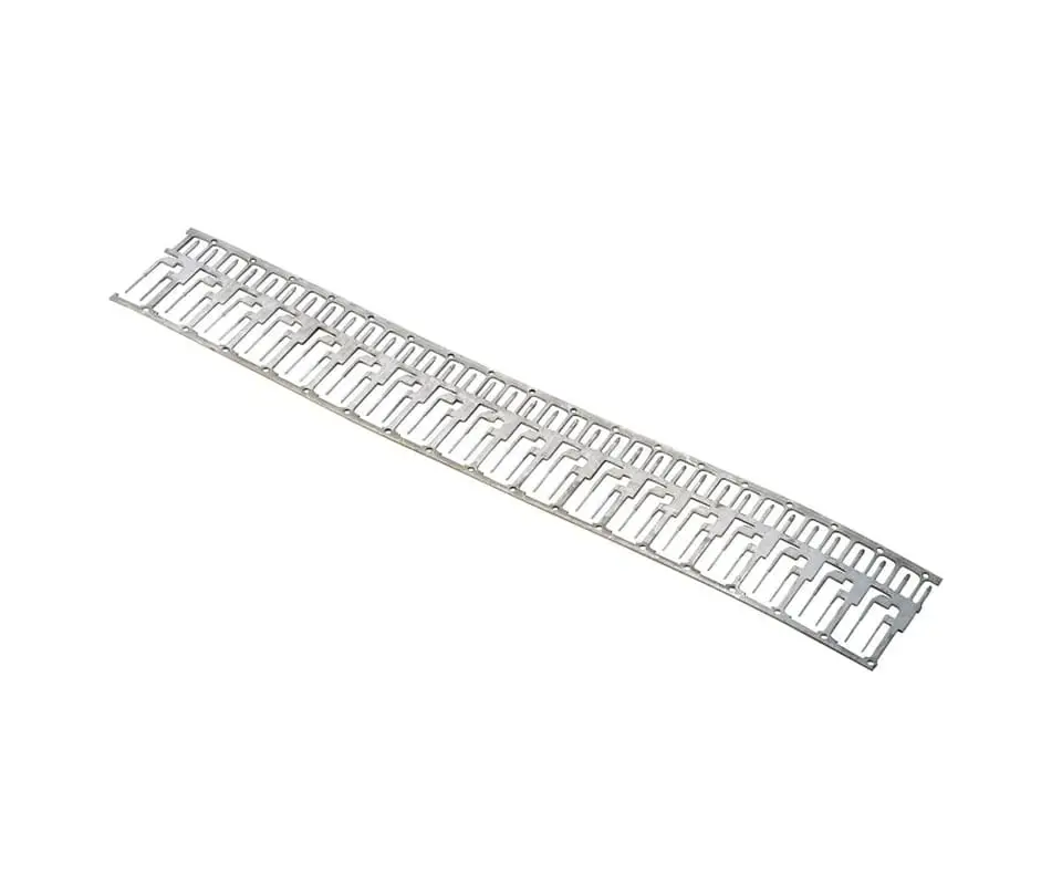
The terminal material must be phosphor bronze C51000 at 0.08–0.12 mm thickness — thin enough to form the tight bend radii required for the compact connector profile, thick enough to maintain the spring force through 100 mating cycles.
The stamping die clearance at this thickness is 5–8 µm, a gap that requires carbide tooling and in-die optical verification of the punch-to-die alignment at every tool maintenance interval.
USB-C connector terminals have become the highest-volume precision terminal in consumer electronics. A single USB-C receptacle contains 24 terminals at 0.5 mm pitch, with the power terminals rated for 5 A continuous and the high-speed data terminals carrying 10 Gbps signals.
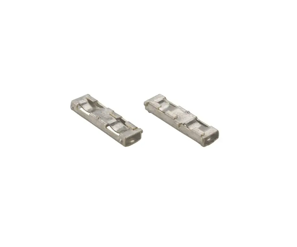
The terminal’s dual-row cantilever beam design must provide 0.3–0.6 N of normal force on the plug contact while surviving 10,000 insertion cycles — a requirement that drives material selection to beryllium copper C17200 for the spring beams, with the cost increment over phosphor bronze justified by the 10× cycle life improvement.
The gold plating on the contact zone must be 0.75 µm minimum over 1.25 µm nickel to survive the full 10,000-cycle life without wearing through to the nickel underlayer, which would increase contact resistance from 30 milliohms to over 100 milliohms.
Industrial I/O and Mating Durability
Industrial I/O connectors for electronics industry applications like PLC modules and sensor interfaces add a mechanical robustness requirement absent from consumer connectors. A terminal inside an M12 circular connector must survive the same electrical requirements as a USB-C terminal while also withstanding the 3 N·m tightening torque applied to the connector’s threaded coupling ring — a force that transmits through the connector body and can shift the terminal’s position relative to the PCB by 0.05–0.10 mm if the terminal’s board-mount section lacks a positive retention feature in the connector housing.
[Compliance Anchor]: Connector terminals for applications exceeding 5 Gbps data rates must undergo time-domain reflectometry verification on the production connector assembly to detect impedance discontinuities exceeding 10 ohms from the nominal differential impedance, with fails traced to terminal geometry deviations using cross-sectional metallography of the suspect terminal position.
💡 Material Selection for High-Cycle Applications: Phosphor bronze C51000 provides adequate spring force retention through 100 cycles, but applications exceeding 500 cycles demand beryllium copper C17200 — the 3× material cost must be weighed against field failure risk in consumer devices. submit your mating cycle requirement for a material recommendation with spring force retention data.
High-Volume Process Control
In-Die Vision Inspection and Reel-to-Reel Plating
Electronics terminal production at volumes of 10–100 million units per year demands a different approach to quality assurance than the statistical sampling used in aerospace or medical. At 50 million terminals per year and a target defect rate of 10 PPM, 500 defective terminals escape to the customer annually.
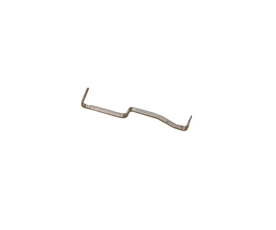
In-line vision inspection at multiple stations within the progressive die provides the detection capability: a camera positioned after the forming station captures the terminal’s profile and measures bend angles, lead coplanarity, and cut-off length. A second camera after the plating cell verifies the plating coverage at the contact zone. Terminals that fail any inspection are marked with a laser and diverted at the final cut-off station, preventing them from reaching the reel.
Reel-to-reel plating forms the backbone of high-speed electronics terminal manufacturing. The terminal strip exits the stamping die at 10–30 meters per minute and enters a selective plating line where the contact zone receives gold plating through a precision mask that limits the gold to the functional contact area — typically 1–3 mm of the terminal length.
The remainder of the terminal, including the SMT lead and the retention feature, receives tin plating for solderability. This selective approach reduces gold consumption by 70–80% compared to full-body gold plating, cutting the terminal cost by $0.002–$0.005 per piece — a margin-critical difference in consumer electronics where connector costs are measured in fractions of a cent.
[Compliance Anchor]: High-volume electronics terminal production must demonstrate process capability Cpk ≥1.67 for critical characteristics over a minimum of 3 production lots per ANSI/ASQ Z1.4, with ongoing SPC monitoring using X-bar and R charts that detect tooling wear trends before they produce out-of-spec terminals — waiting for a QC inspection failure to trigger corrective action guarantees nonconforming material reaches the customer at production volumes above 1 million units per month.
Compliance Pass
Terminals passing contact resistance testing can ship with coplanarity drift from a single production shift, producing a 2% open-circuit rate that triggers PCB line stops. Kravzik stamps electronics-grade terminals on carbide progressive dies with in-die vision inspection, delivering Cpk ≥1.67 with coplanarity and solderability data per reel.
Send us your connector requirements for an electronics qualification data package, including Cpk process capability data and J-STD-002 solderability reports.
Related Engineering Resources
- Phosphor bronze C51000 fatigue properties and spring force retention data in copper alloy material property reference
- Selective gold plating for fine-pitch connector terminals in gold and silver plating process capabilities
- Carbide progressive die tooling for high-volume electronics terminal production in progressive die tooling services